Original Link: https://www.anandtech.com/show/2493
Intel's Atom Architecture: The Journey Begins
by Anand Lal Shimpi on April 2, 2008 12:05 AM EST- Posted in
- CPUs
The Atom processor's architecture is not about being the fastest, but being good enough for the tasks at hand. A product like ASUS' EeePC would not have existed 5 years ago, the base level of system performance simply wasn't great enough. These days, there's still a need for faster systems but there's also room for systems that aren't pushing the envelope but are fast enough for what they need to do.
The complexity of tasks like composing emails, web browsing and viewing documents is increasing, but not at the rate that CPU performance is. The fact that our hardware is so greatly outpacing the demands of some of our software leaves room for a new class of "good enough" hardware. So far we've seen a few companies, such as ASUS, take advantage of this trend but inevitably Intel would join the race.
One of my favorite movies as a kid was Back to the Future. I loved the first two movies, and naturally as a kid into video games, cars and technology my favorite was the second movie. In Back to the Future II our hero, Marty McFly, journeys to the future to stop his future son from getting thrown in jail and ruining the family. While in the future he foolishly purchases a sports almanac and attempts to take it back in time with him. The idea being that armed with knowledge from the future, he could make better (in this case, more profitable) decisions in the past.
I'll stop the analogy there because it ends up turning out horribly for Marty, but the last sentence sums up Intel's approach with the Atom processor. Imagine if Intel could go back and remake the original Pentium processor, with everything its engineers have learned in the past 15 years and build it on a very small, very cool 45nm manufacturing process. We've spent the past two decades worrying about building the fastest microprocessors, it turns out that now we're able to build some very impressive fast enough microprocessors.
The chart below tells an important story:
| Manufacturing Process | Transistor Count | Die Size | |
| Intel Pentium (P5) | 0.80µm | 3.1M | 294 mm^2 |
| Intel Pentium Pro (P6) | 0.50µm | 5.5M* | 306 mm^2* |
| Intel Pentium 4 | 0.18µm | 42M | 217 mm^2 |
| Intel Core 2 Duo | 65nm (0.065µm) | 291M | 143 mm^2 |
| Intel Core 2 Duo (Penryn) | 45 nm | 410M | 107 mm^2 |
In 1993, it took a great deal of work for Intel to cram 3.1 million transistors onto a near 300 mm^2 die to make the original Pentium processor. These days, Intel manufacturers millions of Core 2 Duo processors each made up of 410 million transistors (over 130 times the transistor count of the original Pentium) in an area around 1/3 the size.
Intel isn't stopping with Core 2, Nehalem will offer even greater performance and push transistor counts even further. By the end of the decade we'll be looking at over a billion transistors in desktop microprocessors. What's interesting however isn't just what Intel can do to push the envelope on the high end, but rather what Intel can now do with simpler designs on the low end.
What's possible today on 45nm...
With a 294 mm^2 die size, Intel could not manufacture the original Pentium for use in low cost devices however, today things are a bit different. Intel doesn't manufacture chips on a gigantic 0.80µm process, we're at the beginnings of a transition to 45nm. If left unchanged, Intel could make the original Pentium on its latest 45nm process with a die size of less than 3 mm^2. Things get even more interesting if you consider that Intel has learned quite a bit in the past 15 years since the debut of the original Pentium. Imagine what it could do with a relatively simple x86 architecture now.
Intel Aims at the Mainstream
 We can easily make arguments for faster processors in most desktops and notebooks, but we're on the verge of computing being far more ubiquitous than that. Our desktops and notebooks have gotten so fast that we demand similar functionality and responsiveness from all electronic devices we use on a regular basis. The most frustrating until recently was the smartphone; smartphones have become more complex in the types of tasks we require of them, yet their interfaces have hardly given us the PC-experience we're used to. Apple attempted to change this with the iPhone but there's still much room for improvement. We've seen the same sorts of problems on more conventional consumer electronics. Blu-ray players that cost as much as PCs yet take longer to boot up and are beyond sluggish when interacting with menus. We can run Half Life 2 at 200 fps but we can't make the UI on a TV respond quickly to button presses on a remote control?
The problem is that most of the CE industry is quite commoditized and we're quickly headed for a world where LCDs become cheap enough that it makes sense to have multiple surfaces in a room that can act as displays. There's no room for a powerful CPU that costs hundreds of dollars in TVs, Blu-ray players or even simpler devices like portable GPS units.
The processing power required by the interface on a television, the software stack on a GPS, or even the non-decoding components of a Blu-ray player can easily be handled by even the cheapest desktop processors. The question isn't "can we" make these devices faster, it's what's the bare minimum CPU we need to make them faster.
Such a CPU would have to be low power, low cost but without sacrificing performance.
You could argue that the sorts of applications we're talking about can easily be satisfied by something as slow as a Pentium III, or maybe even the first Pentium M perhaps? And this is where Moore's law comes into play.
A few years ago, the Pentium III, Pentium 4 and Pentium M were all just as expensive to make as today's Core 2 Duo processors. These days their transistor counts pale in comparison to the 400 - 800 million we're talking about on desktop CPUs. Within 2 years we'll be at over 1 billion transistors on a desktop CPU that costs less to manufacture than the original Pentium processor. But if we looked at it from another angle - is it possible to build a microprocessor that offers the performance of the original Pentium M but make it cheap enough to use in commoditized consumer electronics and make it low power enough to be run without a heatsink?
What AMD Taught Me: x86 Everywhere
Back when AMD first announced its intentions to extend the x86 ISA to 64-bits I asked Fred Weber, AMD's old CTO, whether it really made sense to extend x86 or if Intel made the right move with Itanium and its brand new ISA. His response made sense at the time, but I didn't quite understand the magnitude of what he was saying.
Fred said that the overhead of maintaining x86 compatibility was negligible, at the time around 10% of the die was the x86 decoder and that percentage would only shrink over time. We're now at around 8x the transistor count of the K8 processor that Fred was talking about back then and the cost of maintaining x86 backwards compatibility has shrunk to a very small number. But the benefit of backwards compatibility is huge.
These days just about everything is written for x86, everything in the PC space that is. The consumer electronics world isn't quite as blessed. We're starting to see an increasing number of PC applications asked to run on CE devices, things like web browsers, email clients, or simple network media players. Unfortunately, these CE devices don't run x86 platforms thus the manufacturers are either forced to port open source applications to their platform or try to develop something comparable in house.
The problem is that, generally speaking, the best applications currently exist on the PC. The last thing we want is for a company like Sony to enter the web browser market, I'd much rather have Firefox or IE on my internet enabled TV, or on my touch screen in my kitchen. Sure it can be ported to any architecture, but software developers don't exactly like supporting multiple platforms - it takes a lot of time to debug and maintain, and ends up costing a great deal of money.
The concept Fred was trying to get me to understand back in 2002 was this idea of having x86 everywhere. The instruction set didn't matter, what mattered was being able to run the same code on virtually any device. I've always pointed out that Apple must have hated making the iPhone because it became the only computer-like device in its product lineup that didn't run x86. It meant Apple had to maintain a completely separate software stack, specifically for the iPhone.

Fred was right. As computers infiltrate our homes in less conventional ways, being able to run the same applications on all devices will become increasingly more important.
What's ironic is that while Fred Weber first illuminated this issue for me, it would be Intel that was first to act on it.
A Prelude to Success
This all started back in 2004, in Austin, Texas. Despite the location, I am talking about Intel and not AMD. In 2004, Intel's Austin Design Center was hard at work on another member of the Pentium 4 processor family - codenamed Tejas.
Tejas was scheduled to arrive after Prescott and continue the NetBurst lineage, but as history would have it, Tejas never saw the light of day. The project was canceled and Intel's corporate attention was instead shifted to taking the Pentium M architecture and improving it to be desktop-worthy.
The Tejas team was, as you'd expect, not particularly pleased with their project being canceled. But, as seems to be the case with Intel's best engineers and canceled projects, they channeled their disappointment into passion and excitement for their next design.
I should stop the story here and point out the striking similarity to another Intel success story, that of the original Centrino. Banias was the first Centrino processor, later named the Pentium M. The team that worked on Banias was the same team that worked on Timna, yet another project cancelled very late in the process. After Timna was cancelled the team, working out of Intel's Israel Design Center, went into a brief collective depression for about a month before receiving instructions to work on Banias. Instead of producing something mediocre, the team felt a need to prove something to those who cancelled their beloved Timna project. The result was Banias, which became the Pentium M, led to the Core Duo and eventually gave us the Core 2 family of processors that we love so dearly today.
Back to Austin. We've got a very small team of people who were hard at work on Tejas and now without anything to do. The same sense of proving their worth brew and in 2004 the team received new orders.
The task was to develop a low power, IA (Intel Architecture, read: x86) core for use in a many-core CPU design. Since this core would be used in a many-core CPU, it would have to be very, very low power (you can't have 10s of cores each consuming 100W).
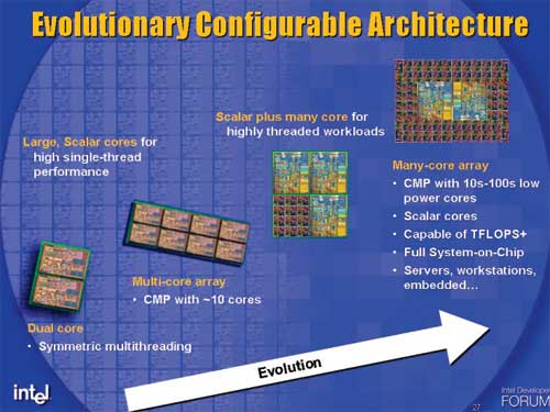
Many-core CPU designs are in Intel's future, Atom has its roots in the many-core initiative
I asked the design team in Austin if this was a dirty joke played on them by upper management - going from a very power hungry design like Tejas to something that would consume a couple of watts. Apparently during Tejas' design, a smaller team in Austin was doing some pathfinding work, looking at very low power simple cores. Since they spent about a year doing this pathfinding work, the transition from Tejas to something very low power was natural despite what it may seem from the outside.
Many of the architects that would work on this new, low power core actually came from other microprocessor companies. Belli Kuttanna, the chief architect on the core, worked for Sun on SPARC processors as well as Motorola designing elements of PowerPC cores. Belli worked with others from Sun and Motorola, but now all under the Intel umbrella. One of the members of the validation team working on the core was also a former AMDer.
Early 2004 was the inception of the pathfinding effort to investigate what would be necessary to develop this new low power core. The codename for this core was Bonnell, which as I've mentioned before is the tallest mountain in Austin, measuring only 750 ft. The petite mountain was a perfect fit for this new, small core (engineers aren't the most creative with naming ;)).
The first step in the pathfinding effort was to find out if Bonnell could be based on an existing Intel microarchitecture. The small team looked at reusing the Pentium M or the yet-to-be-released Core 2 and some analysis was done on both of these options. It didn't take long to come to the conclusion that it wasn't possible to hit the power and performance targets using an existing design. As Intel discovered with Centrino, in order to target a new market it would need to use a new microprocessor design.
The team went back to a clean sheet of paper and started with the simplest of microprocessor architectures, a single-issue, in-order core and built up from there. The designers kept iterating until the performance and power targets at that time were met. You have to keep in mind that in 2004, even Intel didn't have a good idea of exactly where this core would be used. Imagine going back to 2004 and being expected to design the microprocessor architecture that could eventually be used in something like a third generation iPhone - it's borderline impossible.
By the end of 2004, Paul Otellini gave the Austin team specific direction that the Bonnell core would be used in a standalone CPU - not as a part of a many-core design effort. This CPU would be used in UMPCs (Ultra Mobile PCs) and an even more unheard of creation called a MID (Mobile Internet Device). The many-core designs are still under development and I suspect that the first one we'll see come to fruition is a little gem called Larrabee.
Bonnell was just a core, but when combined with a L2 cache and an external bus interface it became the CPU known internally as Silverthorne. More recently, Intel gave Silverthorne a proper name and called it the Atom processor.
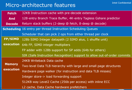
Atom at a Glance
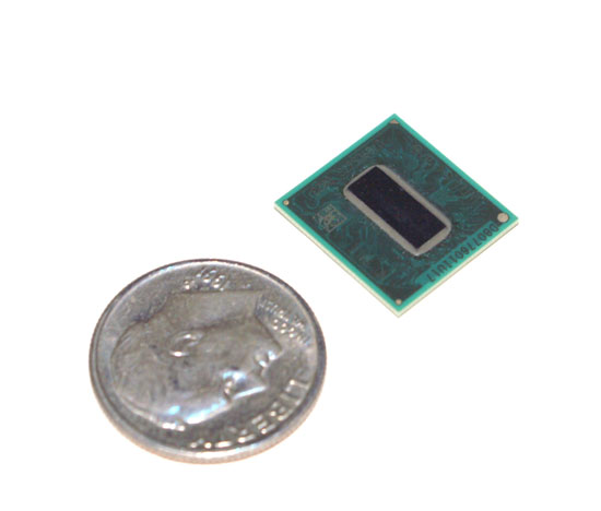
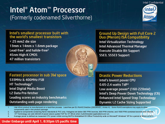
Built on Intel's 45nm manufacturing process, the Atom is Intel's smallest x86 microprocessor with a < 25 mm^2 die size and 13 mm x 14 mm package size. Unlike previous Intel processors that targeted these market segments, Atom is 100% x86 compatible (Merom ISA to be specific, the Penryn SSE4 support isn't there due to die/power constraints).
At a high level, here are some of the architectural features that make the Atom unique. We'll be diving into a few of these over the coming pages:
Intel's Atom: Changing Intel from the Inside
For years at Intel the rule of thumb for power vs. performance was this: a designer could add a feature to a microprocessor design if you get a 1% increase in performance for at most a 2% increase in power. Unfortunately, it's thinking like that which gave us the NetBurst architecture used in the Pentium 4 and its derivatives.
The Intel Atom was the first Intel CPU to redefine the rule of thumb and now the requirement is that a designer may add a feature if it yields a 1% increase in performance for at most a 1% increase in power consumption. It's a pretty revolutionary change and it's one that will be seen in other Intel architectures as well (Nehalem comes to mind), but Atom was the first.
While Atom started as a single-issue, in-order microprocessor the Austin team quickly widened it to be a dual-issue core. The in-order decision stuck however.
Modern day x86 processors can operate on instructions out of program order. It's like if you had to tie your shoe and turn on the TV, you may choose to tie your shoe first and then walk over to the remote control to turn on the TV. You'd complete the quicker task first before moving onto the one that took more time since you didn't have the remote on hand. Processors that are capable of OoOE (Out of Order Execution) work in the same way; when data isn't available in their caches instead of idly waiting on the data, they can execute other instructions that are ready while waiting for the required data to be fetched from memory.
The problem with these out of order processors is that all of this instruction reordering takes up additional die space and increases power consumption. Performances goes up as well but remember, Intel's goal here wasn't to be the fastest, but to be fast enough. Thus the Atom remained an in-order CPU, incapable of executing instructions out of program order and Intel's first in-order x86 core since the original Pentium processor.
The decision to go in-order eliminated the need for much complex, power hungry circuitry. While you get good performance from out-of-order execution, the corresponding increase in scheduling complexity was simply too great for Atom at 45nm. Keep in mind that just as out-of-order execution wasn't feasible on Intel CPUs until the Pentium Pro, there may come a time where transistor size is small enough that it makes sense to implement an OoOE engine on Atom. I don't expect that you'll see such a change in the next 5 years however.
2-Issue and In-Order: Intel's Version of the Cell's PPE
The Austin design team started with a single-issue in-order core but quickly expanded it to be a superscalar, 2-issue design, in other words it is capable of sending up to two instructions down the pipeline at the same time. By comparison most desktop x86 microprocessors are 3 or 4-issue designs.
In order to feed the 2-issue machine, Intel equipped Atom with two decoders. These decoders take instructions fetched from the L1 instruction cache and sequence the series of 1s and 0s into figuring out what the instructions are telling the CPU to do. While the decoders are equal in their ability to decode instructions, there are two paths that an instruction may take: slow and fast.
In the earlier days of the x86 ISA (Instruction Set Architecture) many complained about its support for variable length instructions.
If I tell you that I'm going to give you 2 oranges every 10 seconds, your job becomes much easier than if I tell you that I'm going to give you somewhere between 1 and 3 oranges every 10 seconds. The former would be an example of a fixed length instruction set and the latter a variable length instruction set, unfortunately x86 falls into the realm of the latter.
Atom's slow decoding path does not include any speculative decoding. The instructions are sequenced manually, meaning that each bit is looked at (which takes time) but the instruction is guaranteed to be decoded properly. The instruction is also tagged so that the next time it comes through it can be sent through the fast path.
The fast path obviously employs some speculative decoding and is aided by the tag bit that's set after an instruction goes through the slow path. The slow path yields 1 instruction every 3 clocks, while the fast path can produce 2 instructions every clock.
As Intel learned with Banias (Pentium M), the power penalty for incorrect speculation is unacceptable in a device running on a battery. You'll see a number of tradeoffs where speculative performance tricks are sacrificed in order to maintain low power operation with the Atom processor.
Instructions Gone Wild: Safe Instruction Recognition
The biggest fear with conventional in-order architectures is what happens if you have a high latency instruction that needs a piece of data that isn't available in the caches.
Since in-order microprocessors have to execute the instructions in order, the execution units remain idle until the CPU is able to retrieve the data it needs from main memory - a process that could easily take over a hundred clock cycles. The problem is that during these clock cycles, power is expended but no work is getting done - which is the exact opposite of what we want in an ultra low power microprocessor.
Out of order processors would get around this problem by simply scheduling around the dependent instruction. The scheduler would simply select the next instruction that was ready for execution and work would progress while the data dependent instruction waited for data for main memory. We've already established that a full OoOE core would be too power hungry for Atom, but relying on a pure in-order design also has the potential to be inefficient. Intel's Austin team found a clever middle ground for Atom.
It's called the Safe Instruction Recognition (SIR) algorithm and it works like this. If Atom is executing a long latency floating point operation followed by a short latency integer op you would traditionally stall until the FP op is complete (as we described above). The SIR algorithm looks at the two instructions and determines whether or not there are any data dependencies between the two (e.g. C = A + B followed by D = C + F), if there aren't then Atom will allow the "younger", shorter latency operation to proceed ahead of the longer FP operation.
SIR addresses a very specific case but it sprinkles a little bit of out-of-order goodness into the Atom's otherwise very strict in-order design. I wouldn't be too surprised if future iterations of Atom expand the situations in which these sort of out-of-order tricks are allowed.
Return of the CISC: Macro-op Execution
The Pentium Pro was Intel's first CPU that finally ended the RISC vs. CISC debates of the early 1990s. To the programmer it was still a x86 CISC machine like every previous Intel processor, but internally once it received its x86 instructions it decoded them into smaller micro-ops to run on a simpler, faster and more efficient RISC core.
By maintaining backwards compatibility with all previous x86 processors Intel was able to leverage one of the major strengths of its CISC architecture (mainly the installed x86 user base) while continuing to evolve by relying on a high performance RISC core.
It turns out that some x86 instructions shouldn't be broken up into smaller micro-ops because they tend to augment each other. With the Pentium M Intel began fusing certain micro-ops into single operations so that they would go down the processor's pipelines atomically, thus saving power and improving efficiency. Intel called this feature micro-op fusion. If two micro-ops were treated as one when going down the pipeline that effectively increased the "width" of the CPU, allowing more instructions to be operated on at once. The internal core was still very much a RISC machine, it was just able to do a little more in certain circumstances.
The Atom takes things one step further and most x86 instructions aren't even broken down into micro-ops internally. As Atom isn't an out-of-order core, it doesn't exactly make sense for it to have tons of micro-ops in flight since it can't reorder them for optimal execution. Furthermore, by keeping most instructions as single operations Intel is able to effectively increase the "width" of Atom.
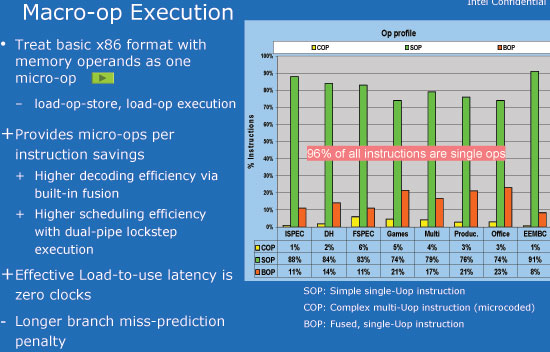
Instructions that are of the format load-op-store or load-op execution are treated as a single micro-op by Atom's decoder. In other words, if you have an instruction that loads data, operates on it, and stores the result - that's now treated as a single micro-op instead of being broken up into three. The benefit being that there's only a single micro-op that's going down the pipeline, leaving room for another one. Atom may only be a 2-issue architecture, but in certain situations it can behave like a much wider machine.
Intel has spent much of the past decade perfecting its ability to break down x86 instructions into smaller, RISC-like operations and building very high performance cores to deal with these small atomic operations. What's most interesting is that we've now come full circle where in the quest for greater performance per watt Intel is now doing the opposite and not breaking down these x86 instructions in many cases.
It Does Multiple Threads Though: The Case for SMT
Despite being 2-issue, it's not always easy to execute two instructions from a single thread in parallel due to data dependencies between the two. Intel's solution to this problem was to enable SMT (Simultaneous Multi-Threading) on Atom (not all models unfortunately) to allow the concurrent execution of up to two threads. Welcome the return of Hyper Threading.
Remember the rule of thumb for power/performance tradeoffs? Intel's decision to enable SMT on Atom was the perfect example of just that. SMT increased power consumption by less than 20% on Atom, however it also yielded a 30 - 50% increase in performance on the in-order core. The decision couldn't be easier.
The Atom has a 32-entry instruction scheduling queue, but when running with SMT enabled each thread has its own 16-entry queue. The scheduler doesn't have to switch between threads each clock, it can do so intelligently, the only limitation is that it can only dispatch 2 ops per clock (since it is a 2-wide machine). If one thread is waiting on data to complete an instruction, on the next clock tick the scheduler can choose to dispatch an op from a separate thread that will hopefully be able to execute.
Making Atom multithreaded made perfect sense from a logical standpoint. The downside to an in-order core is that if there is an instruction that is waiting on data to begin execution the rest of the pipeline stalls while that dependency is resolved. The chances that you'll have two independent instructions from two independent threads both with misses in cache is highly unlikely.
Execution Units
Atom isn't a superwide processor, with an in-order front end and no on-die memory controller it's unlikely that we'll see tremendous instruction throughput. Data dependencies would do a good job of ensuring that tons of execution units remain idle, so Atom's designers did their best to only include the bare minimum when it came to execution units.
There's no dedicated integer multiplier or divider, these functions are shared with the SIMD FP units. There are two SSE units and the scheduler can dispatch either a float or an integer SIMD op to both ports in a given clock.
All of the functional units are 64-bits wide with the exception of supporting full width SIMD integer and single precision FP ADDs.
Fighting Power Consumption...with a Longer Pipeline?
Atom's pipeline is a fairly deep 16 stages, with a 13 stage mispredict penalty. Note that this is longer than the Core 2 Duo's 14 stage pipeline, which is surprising given the low power focus the design team had for Atom.
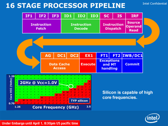
A 16-stage pipeline complete with 3 instruction fetch and 3 instruction decode stages, more than expected
Longer pipelines are generally associated with greater power consumption especially as of late due to the Pentium 4's tenure. Intel gave us three reasons for the long pipeline:
1) Caches
2) Decoder
3) SMT
When faced with a decision between trading off latency for power, the Austin design team always favored keeping power low, even if it meant increasing latencies. Atom doesn't fire the large banks of its caches unless the cache controller knows there's a true hit in the cache, unfortunately this increases the access latency of the cache. In order to keep clock speeds high, these cache accesses have to be further pipelined. The benefit is that power is kept low; Atom keeps things as physically tagged caches to avoid the power burden of a virtually tagged cache.
The same sort of latency tradeoff is made in the decoding stages. Remember the slow vs. fast paths through the decoders? The slow path is higher latency but is guaranteed to properly decode an instruction, the added latency forces Atom to have three decoding stages instead of two.
Finally there are some algorithms in which SMT added a stage or two to the pipeline, the end result being a fairly lengthy pipeline for such a simple CPU. The reasoning however makes sense; there is no NetBurst nonsense here, all of these decisions were made to keep power consumption as low as possible while hitting the right frequency targets. As a fairly simple two-issue core, Atom needs clock speed in order to give us the sort of performance we are expecting of it.
An Unbalanced L1 Cache: We Know Why
The Atom processor is outfitted with fairly large caches, which are quite necessary given its in-order architecture that's very sensitive to high memory latencies. We wrote the following in our initial Atom (Silverthorne) architecture discussion:
"The L1 cache is unusually asymmetric with a 32KB instruction and 24KB data cache, a decision made to optimize for performance, die size, and cost. The L2 cache is an 8-way 512KB design, very similar to what was used in the Core architecture.
While Silverthorne is built entirely on Intel's high-k/metal gate 45nm process, there is one major difference: SRAM cell size. Intel uses a 0.382 um^2 SRAM cell in Silverthorne compared to 0.346 um^2 in Core 2. Each SRAM cell is an 8 transistor design compared to 6 transistors in Core 2. The larger cell size increases the die size of Silverthorne but it draws less power and runs at a lower voltage."
At the time we didn't have a good explanation as to why the Atom's L1 cache wasn't made of equal sized instruction and data caches, which is usually how Intel designs its processors. Since then we have gotten some more insight into the design decision:
Historically, Intel would design a microprocessor for a particular manufacturing process (e.g. 65nm) and shoot for a target voltage, later attempting to lower that voltage when possible. Atom was designed around the absolute minimum voltage the manufacturing process (45nm) was capable of running at and the engineers were left with the task of figuring out what they could do, architecturally, given that requirement.
The perfect example of this approach to design is Atom's L1 instruction and data caches. Originally these two caches were small signal arrays (6 transistors per cell), they were very compact and delivered the performance Intel desired. However during the modeling of the chip Intel noticed that it was a limiter to being able to scale down the operating voltage of the chip.
Instead of bumping up the voltage and sticking with a small signal array, Intel switched to a register file (1 read/1 write port). The cache now had a larger cell size (8 transistors per cell) which increased the area and footprint of the L1 instruction and data caches. The Atom floorplan had issues accommodating the larger sizes so the data cache had to be cut down from 32KB to 24KB in favor of the power benefits. We wondered why Atom had an asymmetrical L1 data and instruction cache (24KB and 32KB respectively, instead of 32KB/32KB) and it turns out that the cause was voltage.
A small signal array design based on a 6T cell has a certain minimum operating voltage, in other words it can retain state until a certain Vmin. In the L2 cache, Intel was able to use a 6T signal array design since it had inline ECC. There were other design decisions at work that prevented Intel from equipping the L1 cache with inline ECC, so the architects needed to go to a larger cell size in order to keep the operating voltage low.
The end result of this sort of a design approach is that the Atom processor is able to operate at its highest performance state (C0) at its minimum operating voltage.
Hardware Prefetchers: So Necessary
Atom features two hardware prefetchers, one that prefetches from the L2 cache into the L1 data cache and one from memory into the L2 cache.
Hardware prefetching is unbelievably important when dealing with an in-order core because as we've mentioned time and time again, not having data available in cache means that the pipelines will stall until that data is available.
The obvious long term solution to the problem of data starvation is to integrate the memory controller on die. With no 45nm MCH design ready by the time the Atom design was complete, Intel has to wait until the second generation Atom (codename: Moorestown) to gain an on-die memory controller.
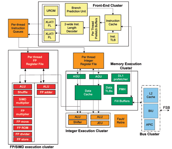
Building by FUBs
Below we have a conventional block diagram of the Intel Atom processor:
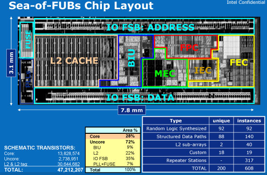
You'll see nine distinct blocks and in conventional microprocessor design at Intel, this is how the chip would be divided and conquered. You'd have one team working on the L2 cache, one team working on the IO interfaces, etc... Unfortunately the team at Austin was significantly smaller than your conventional microprocessor design group, so things had to be done a little differently.
Intel calls the Atom approach a Sea-of-FUBs chip layout, a more granular approach to chip layout and design. A FUB (Functional Unit Block) is a floor-plannable object, an individual adder is a FUB, a decoder is a FUB, a cache is a FUB, etc... Because the size of each FUB made them more manageable, a single designer could handle multiple FUBs. The FUBs were also treated more modularly so that once a FUB was defined, designers can work on the FUB, chip integraters can give it to the layout guys and the timing guys can work in parallel as well. It allows for much more concurrent design than the conventional, more serial approach to chip design.
Approximately 90% of the fubs are built using standard Intel logic cells, minimizing the amount of custom work that needs to be done and decreasing the time to market on a processor like Atom. Minimizing the amount of custom Intel logic also means that it's easier to produce variants of Atom that may incorporate other important features depending on the target market.
The Sea-of-FUBs approach was also driven by a desire to keep power consumption and feature creep to a minimum. Area budgets were developed for each FUB and cluster of FUBs and Intel forced the designers to stick to these budgets. If a designer needed more die space for their FUB they couldn't just take it. A review board was setup where designers would come in and ask to grow their FUB. They were allowed to grow the FUB only if they were able to find another FUB that would shrink to accommodate it. The same thing applied for power.
Gridless Clock Distribution
As you push the frequency limits in large, high performance CPUs like the Core 2, you need to minimize overhead in each clock period so you can do the maximum amount of work. Timing is key.
All functional blocks within a microprocessor operate on the same clock signal. You can think of the clock signal like a metronome or a heart beat; work only happens at every tick of the metronome, every beat of the heart or whenever the clock is logically "1" or "high".
There's a single clock signal that's distributed across the chip, but the more complex the chip and the more times the clock changes per second, the tougher it becomes to just make sure the clock gets to all parts of the chip.
In order to reach the absolute maximum frequencies possible, making sure the clock signal arrives at all parts of the chip at the same time with very little variation becomes increasingly important.
The most effective method of distributing this single clock across the chip is by using a metal grid to distribute this critical signal across a large, complex die. The problem with this metal grid is that although it makes sure the clock gets to all parts of the chip with very little skew, it has a huge capacitance and consumes tremendous amounts of power. Large CPU cores can spend 30 - 35% of their power budget simply on clock distribution. This would obviously not work for Atom.
While the Atom processor needs to run at relatively high frequencies, we're not talking about pushing 4GHz here. Without strenuous frequency requirements, a simpler form of clock distribution is ok. Atom uses a binary tree for clock distribution; the clock signal is sent from the PLL to the point of divergence, then fanned out into multiple trees of inverters and finally distributed vertically from each point of divergence to each FUB.
The binary tree approach significantly reduces the amount of current consumed to the point that less than 10% of Atom's power budget is spent on distributing the clock.
Atom's FSB and Multi-Core Aspirations
All Intel Front Side Buses (FSBs) use Gunning Transistor Logic; it produces a good signal that's clearly capable of reaching incredibly high speeds, presently up to 1600MHz. But remember, Atom isn't about being the fastest, just about being fast enough - leaving some room for improvement here.
A GTL FSB uses on-die termination to deliver a very clean data eye each clock, necessary when operating at very high frequencies. Atom isn't the most data hungry processor in the world and thus it can get by with a 400MHz or 533MHz FSB, thus the GTL FSB ends up being overkill.
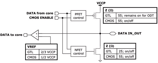
Dual Mode FSB
Atom supports both a GTL or CMOS based FSB, the choice is made during manufacturing and a fuse is blown configuring the FSB for GTL or CMOS operation. When in CMOS mode on-die termination is turned off, the FSB runs at 1/2 the voltage of GTL mode and overall power is reduced. There are no performance tradeoffs to CMOS vs. GTL at the frequencies we're talking about here, the differences are only chipset compatibility and power.
Poulsbo can function in CMOS mode so you can expect Atom processors paired with the Poulsbo chipset to function in this lower power FSB mode. Atom won't be restricted to working with Poulsbo however, and the Diamondville core (Atom for cheap desktops and notebooks) is most likely Atom running in GTL mode so it can work with conventional desktop chipsets.
Atom is multi-core capable but obviously the first incarnation is a single-core design. The first manifestation of a multi-core Atom will be with a dual-core Diamondville due out later this year. Like previous dual-core CPU designs, Atom will place two cores behind a shared FSB. Once it gets an integrated memory controller, the multi-core designs will be more elegant.
Poulsbo: An Unusually Revolutionary Chipset
In 2005 work began on the Poulsbo chipset, the ying to the Atom processor's yang. Much like the Atom processor itself, Poulsbo's design goal was simple: the focus was power and how to reduce it, even if it meant a performance hit.
The lead designers on Poulsbo had all worked on Intel's i840 chipset, one of the only desirable RDRAM chipsets of its time.
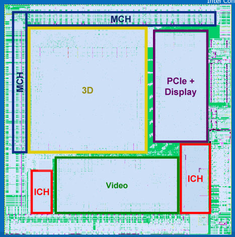
When Poulsbo was designed all of the available ICH designs were 130nm, and thus Poulsbo became 130nm as well. If you look at the pictures of the Atom processor and its chipset, it now makes sense why the chipset is so very huge.
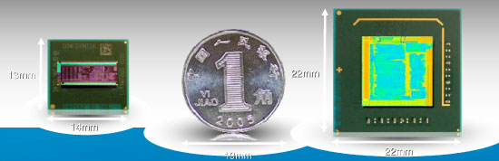
The Intel Atom processor (left) vs. The Poulsbo chipset (right)
With Poulsbo being a 130nm part, it also helps explain why Atom is reserved for larger-than-iPhone devices today: the pair of chips simply wouldn't fit in anything too small. There are obvious power consumption concerns as well, but physically getting these two into a smartphone-sized device is going to be impossible until the next iteration.
At a high level, Poulsbo looks to be no different than your run of the mill Intel chipset with integrated graphics:
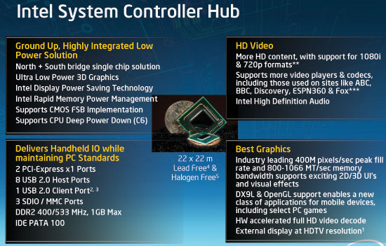
You'll quickly notice that the single chip solution, what Intel is calling a System Controller Hub (SCH) is a bit more unique. Instead of re-using a desktop chipset, Intel architected Poulsbo from scratch. In order to conserve power things like SATA and some of the USB ports were ripped out of the design. The designers chose to move back to PATA mostly because of power and smaller drives. Apparently in an idle state there isn't a power difference between PATA and SATA, but when actively transferring data SATA consumes much higher power due to its serial nature.
The FSB and memory frequencies are locked together which reduces power and PLL count. The chipset features a single channel DDR2-400/533 memory controller.
Poulsbo supports HD audio (Azalia, not the HD audio codecs) but reduced the number of audio engines supported in order to keep power under control. Only 2 channel audio is supported but you can access the audio interface externally, so conceivably you could dock an Atom device (such as a MID) and using an external codec get full 7.1 support.
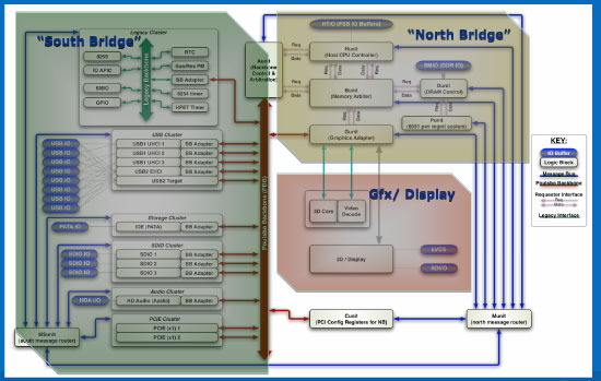
The parts of Poulsbo
Intel also developed a fairly sophisticated message fabric to send data across the SCH - think of it as an on-chip Ethernet network for carrying things like interrupts and power management signals across the chip in an efficient manner.
Poulsbo introduces a new FSB to memory bridge that's much simpler than conventional designs. In most chipsets you have many different queues for traffic between the FSB and memory subsystem designed to extract the best possible performance from the platform. With Poulsbo the designers simply outfitted the memory controller with a large 8K memory and all FSB/memory traffic must go through that. The single memory storage made validation a lot easier, the chipset itself a lot smaller but could incur a performance hit. The MCH/North Bridge part of the SCH is around 20% of the area of what traditional MCH/North Bridges are thanks to this approach.
The ICH/South Bridge parts of Poulsbo are similarly trimmed. Years of legacy have been stripped out of the chipset, there's no parallel port, no floppy disk controller. In mainstream chipsets as long as someone is using the feature, it must be kept in play - the same wasn't true for Poulsbo. If the target market didn't need it, the feature wasn't going in the chipset.
The benefit of cutting the fat in Poulsbo is that the chipset was physically smaller with fewer gates, meaning lower leakage power.
In a highly atypical move for Intel, Poulsbo also supports non-standard 1.5V DDR2 memory. There's no official JEDEC spec for 1.5V DDR2 memory but many vendors have good enough modules that will work at 1.5V, so if an OEM wants to undervolt its memory the chipset will support it.
Much of the Poulsbo's design couldn't have been done had it not been for the Atom project. There are many revolutionary techniques at work within Poulsbo, it's a more modular design, a more efficient design and potentially holds the key to better chipset design in general - but none of these techniques were ever allowed to surface before.
Intel's chipset business is like a clock, every year a new platform is expected and some of the more revolutionary changes that could potentially interrupt the normal flow of things are generally frowned upon. Poulsbo, at least internally, broke down a lot of these barriers. While it's far from the highest performance chipset Intel has ever produced, Poulsbo requires roughly half the power of mainstream chipsets. Intel has been on an efficiency kick with its CPUs for a few years now, Poulsbo may help ignite a similar trend with chipsets as well.
Poulsbo's Graphics: Full HD Decode and not Made by Intel
The graphics core used in Poulsbo is actually not designed by Intel. While Intel wouldn't reveal the true designer, it did confirm that the core was made architected by and licensed from a 3rd party. We asked why and Intel simply stated that this 3rd party was further along in developing a very low power graphics core, and it simply made sense to license it rather than produce its own. This is a significant departure from Intel's standard operating procedures when it comes to integrated graphics in its chipsets, and highlights how very different the Atom project was from previous designs.
Update: Imagination Technologies has announced that Intel uses the PowerVR SGX graphics core and the VXD HD video engine.
The 3D block of Poulsbo was designed by Imagination Technologies
The graphics core does include a full HD video decode engine that can fully accelerate H.264, MPEG-2 and VC-1 video streams. Intel claims that the engine is capable of decoding full bitrate Blu-ray movies however it lacks the ability to decode a second stream, and thus can't be certified for use in a Blu-ray device. Intel claims that the platform will only consume 120mW during H.264 decode.
Then there's the issue of output resolution. The graphics engine only allows a 1366 x 768 output resolution, so while it can decode a full 1080p HD stream, it can only output it at a lower resolution.
On the 3D side Poulsbo's GPU is said to support both DX9 and DX10, but the initial driver will only support DX9L. Honestly, in situations like these we'd be surprised to see anything beyond the initial level of graphics support. GPU performance isn't going to be anything tremendous but we did see Poulsbo running UT2004 quite well in a live demo. Intel told us to expect a 3DMark '05 score around the 150 point mark.
The 2D engine in Poulsbo is still an Intel designed block.
Lower Power than Centrino
(This page is taken from our earlier look at the Intel Atom architecture)
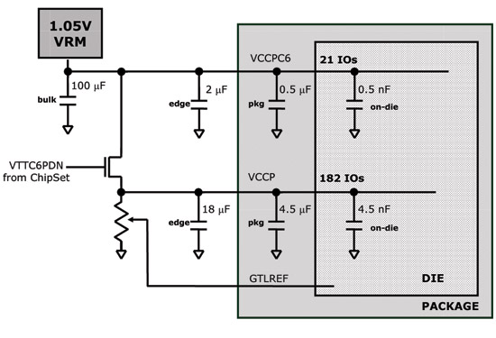
With mobile Penryn Intel introduced a new power state it calls C6. In the C6 power state the CPU is in a virtual reset state, and core voltage is very close to zero. The core clock, all of the PLLs, and caches are completely turned off. All of the state data is saved in a 10.5KB storage area, similar to mobile Penryn (but smaller since there's not as much state to save). Upon exiting C6 the processor's previous state is restored from this memory, called the C6 array. It takes around 100us to get out of C6, but the power savings are more than worth the effort - it's a similar approach of power for performance that we saw in the design of the original Pentium M processor.
Clock gating (sending the clock signal through a logic gate that can disable it on the fly, thus shutting off whatever the clock connects to) is an obvious aspect of Atom's design. All Intel processors use clock gating; Atom simply uses it more aggressively - the clock going to every "power zone" is gated, something that isn't the case in mobile Core 2. Each logic cluster (205 total) in Atom is referred to as a Functional Unit Block (FUB) and the entire chip uses what Intel calls a sea of FUB design. Each FUB is clock gated and can be disabled independently to optimize for power consumption. The cache in Atom is in its own FUB, which apparently isn't the case in mobile Core 2.
Keeping Silverthorne on life support, only 21 pins are necessary
Atom uses a split power plane; in its deepest sleep state (C6) the chip can shut off all but 21 pins which are driven by the 1.05V VRM. By having two separate power planes the chip can manage power on a more granular level. While it can't disable individual pins, it can disable large groups of them leaving only 21 active when things like the L2 cache and bus interface are powered down.
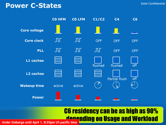
Intel mentioned that Atom will remain in its C6 sleep state 90% of the time. However, that figure is slightly misleading because it's only possible to remain in C6 when the CPU is completely idle. The 90% figure comes from taking into account a mobile device sitting in your pocket doing nothing most of the time. When in use, Atom won't be able to spend nearly that much time in C6.
Despite the implementation of a C6 power state, Atom will still lose to ARM based processors in both active and idle power. The active power disadvantage will be erased over the coming years as the microarchitecture evolves (and smaller manufacturing processes are implemented), while the idle power requires more of a platform approach. As we reported in our first Menlow/Silverthorne article:
"The idle power reduction will come through highly integrated platforms, like what we're describing with Moorestown. By getting rid of the PCI bus and replacing it with Intel's own custom low-power interface, Intel hopes to get idle power under control. The idea is that I/O ports will only be woken up when needed (similar to how the data lines on the Centrino FSB function), and what will result are platforms with multiple days of battery life when playing back music."
Performance Expectations
Intel revealed some early performance data of Atom comparing it to an ARM11 core and using web page render times as the benchmark of choice:
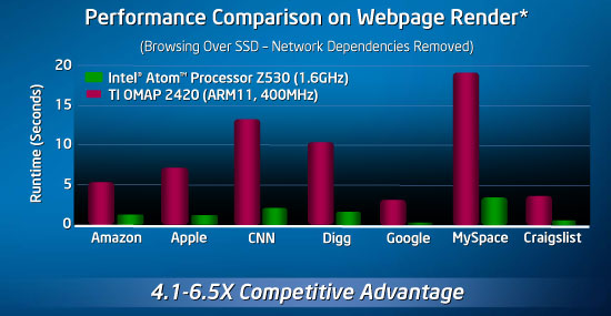
The performance advantage, at least according to Intel's data, is quite clear. While not depicted here, Intel claims to be around 2x the speed of the ARM CPU in the iPhone which is a significant advantage.
What isn't shown here however is a comparison of power consumption or form factor, both areas that ARM currently holds the advantage in. The fact of the matter is that while Atom today is faster than competing ARM offerings, it plays in a completely different space. ARM based products boast smaller form factors and draw less power.
Intel has consistently made the claim that Atom would offer the performance of the first Pentium M at significantly lower power. We were finally able to put that to the test when Intel shared some preliminary data with us. Under SYSMark 2004, a 1.6GHz Atom is around 20% faster than an 800MHz Pentium M (90nm Dothan). As you can expect, a 900MHz Atom is slower than the 800MHz Pentium M as it needs clock speed to make up for the low IPC of the in-order core.
What's even more impressive is the Atom test platform I saw running. Intel showed me an Atom test motherboard running Windows Vista and Unreal Tournament 2004 at smooth frame rates, without so much as a heatsink on the CPU. The surface of the CPU was around 35C and it did not even need a heatsink.
While I'm still not very positive on the first Atom devices, this was the one live demo that honestly had me impressed. It's been far too long since the days when serious CPUs didn't need heatsinks, and it looks like with Atom - Intel may just be bringing that back.
The Product Lineup
Alongside the technology disclosure, Intel is also unveiling the first five Atom processors that will be shipping this year:
| Clock Speed | TDP | Average Power | Idle Power (C6) | FSB | SMT | Price | |
| Intel Atom Z500 | 800MHz | 0.65W | 160mW | 80mW | 400MHz | No | $45 |
| Intel Atom Z510 | 1.1GHz | 2W | 220mW | 100mW | 400MHz | No | $45 |
| Intel Atom Z520 | 1.33GHz | 2W | 220mW | 100mW | 533MHz | Yes | $65 |
| Intel Atom Z530 | 1.60GHz | 2W | 220mW | 100mW | 533MHz | Yes | $95 |
| Intel Atom Z540 | 1.86GHz | 2.4W | 220mW | 100mW | 533MHz | Yes | $160 |
We originally expected Atom to top out at 1.60GHz but it looks like Intel wanted an even higher performing 1.86GHz part in the mix. At 1.86GHz, the Atom should offer performance beyond that of a 1.0GHz Pentium M - not bad for having a 2.4W TDP.
The pricing is admittedly higher than expected, at least for the chips with Hyper Threading (SMT) enabled. Given that the Atom processor is effectively targeting UMPCs and MIDs, the pricing structure makes sense but in order to get x86 everywhere Intel is going to need to offer higher performance at its lower price points.
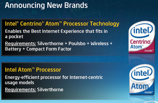
Centrino Atom
As we've reported before, along with the Intel Atom brand comes the new Centrino Atom brand. The requirements are as follows:
Final Words
Over the next six months we will begin seeing the first devices based on Intel's Atom processor. For 2008, Intel expects to see Atom used primarily in 5" form factor MIDs (Mobile Internet Devices). I've played with prototypes of these Atom based MIDs and honestly, they are not any more impressive than the UMPCs that preceded them. The interfaces are sluggish, the devices are still too bulky and I'm not completely convinced that they're worth the added hassle of carrying one around with me all day.
Intel seems to think that Atom based portable GPS devices will be some of the more interesting devices out this year, and while I see some potential there I'm just not that excited.
It's a shame because I am quite excited about the Atom processor, or its future to be more specific. I'm honestly fed up with poor performance in just about every consumer electronics device that I live with - I want the sort of responsiveness that I get with my desktop or notebook, but I want that in my cable box, in my TVs, mobile phones, Blu-ray players, toasters, etc...
The first iteration of Atom simply won't deliver on enough fronts to make the sort of revolutionary changes I want. It lacks the level of integration necessary for truly portable devices and where I really want to see it isn't in bulky MIDs and UMPCs, but rather in things like the iPhone.
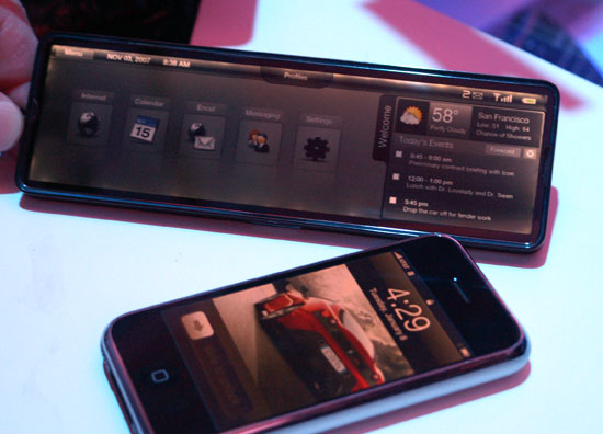
The iPhone (bottom) and a mockup of what the Atom could be in within 3 years (top)
I don't have high expectations for Atom today, while it will surely enable even more EeePC-like devices it's the processor's future that I'm most interested in - and Intel is too. You can find Intel silicon in the majority of desktop and notebook PCs shipped, but if Intel were able to make Atom a success you would find Intel in much, much more. TVs, phones, set top boxes, MIDs, all of these would be running x86 and potentially Intel processors. We always wondered what Intel would do to its spare fab capacity if it integrated a north bridge/memory controller onto its CPUs, with Atom we now have that answer.
The beauty of Atom being successful in these markets is that it doesn't just benefit Intel but AMD and the markets as a whole. Intel will be in for a fight once it begins competing with ARM based processors for space in the CE market, which should promote competition. In those areas where Intel does manage to bring x86 where it hasn't been before, those will quickly become areas where AMD can offer an Atom alternative. Remember that AMD built much of its CPU business on offering a more cost effective x86 alternative to Intel; there's no reason to believe that the same trend won't continue should Atom become successful in the CE industry.
Competition is a very good thing and it's rare that Intel plays the underdog in an industry, but with Atom it most definitely is. The road ahead will be a long one for Intel and its new baby, but the future does look very bright:
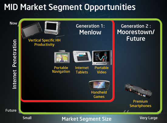
What made Atom possible is also what will make it better over time. Moore's law should mean some very interesting things are in store for the processor. The Moorestown update will bring about a more integrated solution, finally enabling Atom to find its way into larger smart phones.
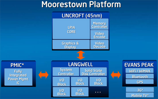
Moorestown will bring an integrated memory controller to Atom among other things...
Take things one step further with an eventual 32nm shrink of Moorestown in the 2011/2012 timeframe and I think we may just be able to have x86 everywhere at the start of the next decade.


